Micro Micro Vias: The Key to High-Density Interconnects
As technology advances, the demand for smaller, faster, and more efficient electronics continues to grow. One of the key components that enables this miniaturization is the micro micro via, a small, round hole in a printed circuit board (PCB) that facilitates high-density interconnections. In this article, we will delve into the world of micro micro vias, exploring their advantages, applications, and manufacturing processes.
What are Micro Micro Vias?
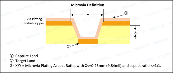
A micro micro via, also known as a microvia or laser via, is a small-diameter hole in a PCB that connects different layers of the board. Typically, micro vias are less than 150 micrometers in diameter and have a maximum aspect ratio of 1:1. These miniature connections play a vital role in creating more compact and efficient circuit designs, particularly in high-density interconnect (HDI) boards.
Advantages of Micro Micro Vias
- Increased Density and Miniaturization: Micro vias enable high-density interconnections, allowing designers to create compact layouts and integrate more components in a limited space.
- Improved Signal Integrity: Micro vias help in impedance matching, ensuring that signal reflections and losses are minimized.
- Lower Parasitic Capacitance: Micro vias have a lower parasitic capacitance compared to traditional vias, making them ideal for high-speed circuits.
- Flexibility and Versatility: Micro vias can be placed anywhere on the PCB, making them suitable for a wide range of applications.
Applications of Micro Micro Vias
Micro vias are used in a variety of applications, including:
- High-Density Interconnect (HDI) Boards: Micro vias are essential for HDI boards, enabling the creation of densely packed circuits.
- High-Speed Circuits: Micro vias are ideal for high-speed circuits, where signal integrity and low parasitic capacitance are critical.
- Power and Signal Circuits: Micro vias are used in power and signal circuits to reduce crosstalk and improve signal integrity.
- IoT and Wireless Devices: Micro vias are used in IoT and wireless devices, where miniaturization and high-density interconnects are essential.
Manufacturing Processes for Micro Micro Vias
Micro vias are typically created using laser drilling or mechanical processing. Laser drilling is a popular method, as it offers high precision and accuracy, and eliminates the need for drilling residue.
Conclusion
Micro micro vias are a critical component in modern electronics, enabling the creation of high-density interconnects, improving signal integrity, and reducing parasitic capacitance. As technology continues to advance, the demand for micro vias will only grow, making them an essential part of the PCB manufacturing process.
Types of Micro Vias
There are several types of micro vias, including:
- Blind Vias: Vias that connect only one layer to another.
- Buried Vias: Vias that connect multiple layers, but are not accessible from the top or bottom layer.
- Stacked Vias: Vias that are stacked vertically to form a continuous interconnect between layers.
- Staggered Vias: Vias that are staggered or offset from each other, used to increase density and reduce crosstalk.
Future Advancements in Micro Via Technology
As technology advances, we can expect to see new developments in micro via technology, including:
- Nanovias: Smaller vias that can be used in even more compact designs.
- New Materials: New materials with improved properties, such as higher thermal conductivity or better electrical insulation.
- Cost-Effective Manufacturing Processes: New manufacturing processes that reduce costs and increase efficiency.
- Integration with Flexible and 3D-Printed PCBs: The integration of micro vias with flexible and 3D-printed PCBs, enabling new design possibilities and applications.


